Nanofabrication (Part II)
The principal micro- and nanofabrication methods in Nanotechnology
A number of techniques are used for the fabrication of micron-scale devices. Some of these techniques have been adopted from the well-established field of semiconductors, but others have been specifically developed for microfabrication. The microfabrication process utilizes these techniques in a sequential manner to produce the desired structure. These structures can be built within the bulk of a substrate material in what is known as bulk micromachining, or on the surface of the substrate through surface micromachining (Voldman et al 1999). In most cases, however, a combination of bulk and surface micromachining is utilized in the fabrication of the desired system.
The most important microfabrication techniques are photolithography, soft lithography, film deposition, etching, and bonding. Photolithography is used to transfer a user-generated shape onto a material through the selective exposure of a light sensitive polymer. Soft lithography encompasses three different techniques which are all based on the generation and utilization of the mold of a microstructure out of poly(dimethylsiloxane). Film deposition, as its name suggest, consists of the formation of micron-thick films on the surface of a substrate. Etching selectively removes materials from the surface of the microdevice by either chemical or physical processes. Finally, bonding adheres substrates together with or without the use of intermediary layers.
Photolithography
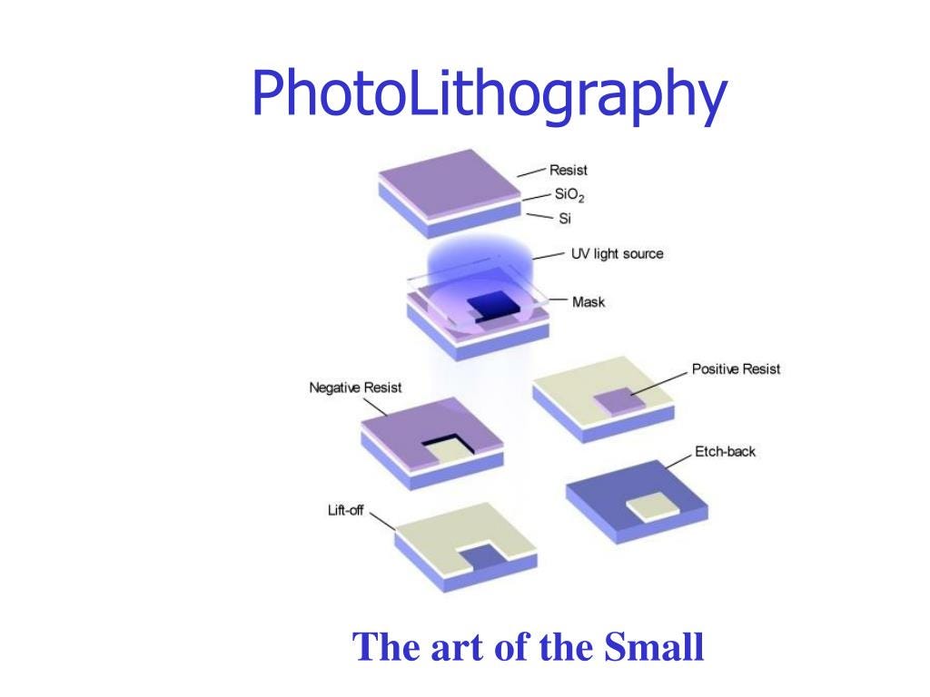
Photolithography is one of the most readily employed microfabrication techniques and is used to create patterns into a material.
In the first step, a substrate material, such as silicone or glass, is coated with a layer of a photoresist, or light-sensitive polymer. A photomask, made by patterning with an opaque material the desired shape on a glass dish or other transparent material, is placed on top of the substrate and photoresist. This assembly is then irradiated with UV light, thus exposing the sections of the photoresist not covered by the opaque regions of the photomask. Depending on the type of photoresist utilized, the photoresist polymer will undergo one of two possible transformations upon exposure to light. When light illuminates a positive photoresist, the exposed regions break down and become more soluble in a developing solution. As a result, the exposed photoresist can be removed when in contact with the developing solution. A negative photoresist, on the other hand, becomes crosslinked upon exposure to light, thus becoming insoluble in the developing solution. Consequently, upon contact with the developing solution, only the parts not exposed to light will be removed.
Soft lithography
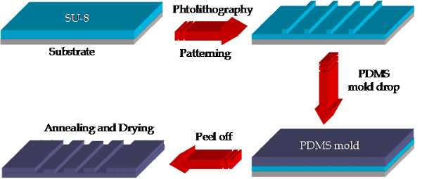
Imagen Courtesy: Fabrication process of PDMS channel. (Shin-Won Kang, School of Electrical Engineering and Computer Science, Kyungpook National University, Republic of Korea)
Soft lithography, similarly to photolithography, is a method also used to transfer a pattern onto a surface. It utilizes a microstructure replica produced by molding a polymer, such as poly(dimethyl siloxane) (PDMS) to a master, which is manufactured through other microfabrication techniques such as photolitography. There are three main soft lithography processes: micro-stamping, stencil patterning, and microfluidic patterning
Film deposition
The application or growth of layers of materials, or films, on the surface of microstructures is a common procedure of microfabrication. Films can play a structural or functional role in the design. For example, they may be used during microfabrication as sacrificial or masking layers that protect the base material from etching, or even as electrical components for a microfabricated device. Numerous types of materials are used for the generation of films. Among these, the most commonly used are plastics, silicon-containing compounds, metals, and biomolecules
Figure shows a schematic that can help in understanding the different processes in a CVD reactor. Chemical vapor deposition processes can be broken down into a number of discrete steps: First the precursor chemicals must be fed into the CVD reactor. Once in the reactor, precursor molecules must be transported to the substrate surface, usually through a combination of fluid transport and diffusion. Once on the surface, the precursor molecule must remain there long enough to react. After reaction occurs, the product thin film atom must remain on the surface while the by-product molecules must desorb from the substrate surface to make room for more incoming precursor molecules.
Etching
Etching is a process that aims to create topographical features on a surface by selective removal of material through physical or chemical means. Etching can be isotropic if it preceeds equally in all directions or anisotropic if it proceeds in one specified direction, isotropic etching occurs not only in the direction of depth, but also laterally, and results in a curved profile. Anisotropic etching, occurs in only in one direction, usually selectively increasing the depth of the cavity.
Courtesy Image: Schematic diagram of nanofabrication process. Masahiko Yoshino (Tokyo Institute of Technology, Japan)
The mechanisms used for etching utilize liquid chemicals or gaseous physico-chemical processes. These two methods are more commonly known as wet etching or dry etching, respectively. Dry anisotropic etching results in a flat profile, while wet anisotropic etching results in cavities with inclined side-walls. The characteristic slanted profile of wet anisotropic etching is a result of the interaction of the etching reagent with the crystalline structure of the material being etched. The crystal structure determines the rate of etching that occurs at each crystal plane. For most applications, the flat profile of dry anisotropic etching is adequate. Reactive ion etching, which utilizes oxygen or fluorine plasma, has also been extensively used.
Bonding
Reversible and irreversible bonds can be formed between microstructures to form tight seals or to obtain desired structures. There are numerous bonding methods available that are specific for the material of interest. For example, irreversible anodic bonding is possible between a silicone substrate and a non-pure glass film. The formation of this bond requires exposure of the system to temperatures in the order of 400°C, high pressure, and an electric field. Fusion bonding, on the other hand, consists of the annealing of two surfaces at high temperatures (∼1000°C)
Image Courtesy: Heat flow during bonding: (a) external and (b) internal. Lutz Hofmann (Fraunhofer Institute for Electronic Nano Systems ENAS | ENAS · Nano device technologies Dr.-Ing, Germany)
Bonding of polymers can be carried out through heating above the glass transition temperature and applying pressure to seal the structures, through laser welding, or ultrasonic welding. In addition, adhesives can also be utilized to bind two materials. However, the addition of intermediate layers will affect the properties of the system and must be taken into account.
Don't hesitate to subscribe if you haven't already done so.
Regards and take care.
Born in 2012, Scixel is a project devoted to the improvement of the scientific comunication through the creation of graphical products: pictures, animations, graphs, posters, etc. Scixel consists of scientists with a deep knowledge in digital graphics but also with a long experience in giving talks, preparing posters and papers and other daily situations of scientific work.
We have focused our work into universities and research institutes all over the world: TuDelft (The Netherlands), NIMS (Japan), Basel University (Switzerland), Universidad Autónoma de Madrid, CNB or ICFO (Spain), to name a few.
Web: https://scixel.es/
If you are a company or an individual who would like to place your advertising in my newsletter you can contact me (email) and let me know your request of type of ad and number of newsletters you would like to place it. I will send you a budget as soon as possible.


