Image Courtesy: The world's smallest guitar is 10 micrometers long -- about the size of a single cell -- with six strings each about 50 nanometers, or 100 atoms, wide. Made by Cornell University researchers from crystalline silicon, it demonstrates a new technology for a new generation of electromechanical devices. You will find more info about this image at the end of the newsletter
What is nanofabrication?
The terms nanofabrication and nanomanufacturing are often used interchangeably for making one-, two-, or three-dimensional nanostructures in various contexts (medical, photonics, electronics, energy, etc.), with a relatively high degree of functionality and structural complexity and hierarchy.
One possible approach to distinguish between the terms is by using the criterion of economic viability: the connotations of industrial scale and profitability associated with the word manufacturing imply that nanomanufacturing is an economic activity with industrial production facilities with more or less fully automated assembly lines. By contrast, nanofabrication is more of a research activity based on developing new materials and processes – it's more a domain of skilled craftsmen and not of mass production.
Today, the only industry where nanoscale manufacturing technologies are employed on a large scale is the semiconductor industry, where device structures have reached the single nanometers scale. Of course, the chemical industry has long been working with nanoscale particles and pigments, but this falls more into the realm of chemistry rather than nanomanufacturing.
There are different ways of fabricating functional nanostructures. The two notions you hear most are top-down and bottom-up methods.
Top-down versus bottom-up nanofabrication
Michelangelo was a top-down artist. He took one big, raw block of Carrara marble and after years of chiseling away produced a spectacular statue like David. In the process he reduced the original block of marble to half its original volume and left the other half as waste.
This is the nanotechnology equivalent of lithography – predominantly photolithography, which is the standard workhorse employed in today's semiconductor industry, and nanoimprint lithography (NIL) for the large-scale production of nanoparticles for diagnostic and therapeutic applications – and other top-down methods where you start by taking a block of material and remove the bits and pieces you don't want until you get the shape and size you do want.
In the process you spend (relatively much) energy, use (sometimes very toxic) chemicals, produce (often quite a bit of) waste, need a lot of patience (these processes are relatively slow) and often the results are quite unique and not easily replicable.
Optical lithography and NIL are the dominant top-down nanomanufacturing methods, although there are a large number of other nanofabrication approaches available. Electron beam lithography (EBL) for instance can generate sub-10 nm features, over large areas, with good placement and overlay, but because of its relatively low throughput, it is limited commercially to the production of masks for use in photo- and nanoimprint lithography and device development.
In contrast to the deterministic nature of top-down processes, bottom-up processes are driven by a combination of thermodynamics and kinetics which then determines the yield of the desired structure.
Bottom-up nanofabrication processes typically don't need expensive tooling to create nanoscale structures, and scaling to large volumes is potentially straightforward. With the application of the tools of chemical synthesis, quantum dots, plasmonically active particles, carbon nanotubes, metallic nanowires, and multifunctional particles for medical applications have been successfully produced in manufacturing quantities.
Self-assembly
The key to using self-assembly as a controlled and directed fabrication process lies in designing the components that are required to self-assemble into desired patterns and functions. Self-assembly reflects information coded – as shape, surface properties, charge, polarizability, magnetic dipole, mass, etc. – in individual components; these characteristics determine the interactions among them.
Unfortunately, spontaneous self-assembly relies heavily on the particles' characteristics. Use different particles, and self-assembly will either form different structures or not occur at all.
On a very small scale you wouldn't even use the term self-assembly but rather chemical synthesis – the processes chemists have refined over many years. However, the stability of covalent bonds enables the synthesis of almost arbitrary configurations of only up to 1000 atoms. Larger molecules, molecular aggregates, and forms of organized matter more extensive than molecules cannot be synthesized bond-by-bond. Self-assembly is one strategy for organizing matter on these larger scales.
This technique can be summarized as follows: We have no clue why certain atoms and molecules self-assemble the way they do, but once we can initiate and control the process we can use it to build structures from the bottom-up – atom by atom.
Self-assembly has become an especially important concept in nanotechnology. As miniaturization reaches the nanoscale, conventional manufacturing technologies fail because it has not been possible yet to build machinery that assembles nanoscale components into functional devices. Until robotic assemblers capable of nanofabrication can be built, self-assembly – together with chemical synthesis – will be the necessary technology to develop for bottom-up fabrication
Self-assembly is also the reason why nanotechnologies have such a profound impact on the chemical industry. One example is the huge area of polymers used for industrial products (think plastics). Chemists are using molecules' tendency to self-align to design molecular structures with specific properties.
DNA-based self-assembly
DNA-based self-assembly offers flexibility in the types of structures that can be produced, based on single-stranded, double-stranded or duplex, and more complex supra-molecular assemblies. One-, two-, and three-dimensional structures can be made, and the ability of other nanoscale objects to be functionalized with DNA, combined with the specificity conferred by complementary sequence recognition, means that DNA can connect and organize disparate nanostructures to make relatively complex constructs, including well-controlled nanoparticle crystal lattices, and even active systems.
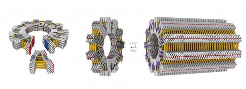
Structural DNA nanotechnology, specifically the molecular self-assembly process known as DNA origami, has emerged as a versatile approach to fabricate nanodevices with complex nanoscale geometry, defined placement of molecular functionalities, and programed mechanical and dynamic properties.
Scientists already are using DNA origami technology to design and build structures on the scale of viruses and cell organelles.
Imagen Courtesy: In a first step, scientists form V-shaped building blocks using DNA-origami techniques. Determined by the opening angle a defined number of building blocks self-assemble into a gear-wheel. In a third step these gear-wheels form tubes with sizes of virus-capsids. (Image: Hendrik Dietz, Technical University of Munich)
DNA origami is a design technique – similar to the traditional Japanese art or technique of folding paper into decorative or representational forms – that is used by nanotechnology researchers to fold DNA strands into something resembling a programmable pegboard on which different nanocomponents can be attached.
These DNA assemblies allow the bottom-up fabrication of complex nanostructures with arbitrary shapes and patterns on a <100 nm scale.
Directed self-assembly – top-down combined with bottom-up. Guided or templated self-assembly typically makes use of boundaries created by top-down methods that interact with a system that has an intrinsic structural length scale. This latter can arise from the balance between long-range magnetic, electrostatic, or strain energy, or, as in the case of block copolymers, can come from local interactions built into the molecular structure of the material.
The technology to fabricate integrated circuits will continue to evolve in capability and cost, but will remain uneconomic for low value-per-unit-area, high-volume products. The family of lithographic technologies, such as nanoimprint, whose development has been driven in large part by the semiconductor industry, will be scaled to suit a variety of cost structures and so will find a wide range of applications, especially for those structures requiring only a single patterned layer.
Bottom-up self-assembly will have a role in the production of simple functional materials that are used in high volumes and must be inexpensive, while directed assembly allows for the imposition of longer-range order and hierarchy that will be important for some applications.
Cover Image:
The world's smallest guitar — carved out of crystalline silicon and no larger than a single cell — has been made at Cornell University to demonstrate a new technology that could have a variety of uses in fiber optics, displays, sensors and electronics.
The "nanoguitar" — made for fun to illustrate the technology — is just one of several structures that Cornell researchers believe are the world's smallest silicon mechanical devices. Researchers made these devices at the Cornell Nanofabrication Facility, bringing microelectromechanical devices, or MEMS, to a new, even smaller scale — the nano-sized world.
The guitar has six strings, each string about 50 nanometers wide, the width of about 100 atoms. If plucked — by an atomic force microscope, for example — the strings would resonate, but at inaudible frequencies. The entire structure is about 10 micrometers long, about the size of a single cell.
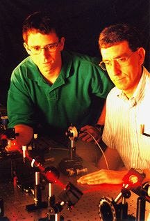
Dustin Carr, left, Cornell graduate student in physics, and Harold Craighead, Cornell professor of applied and engineering physics, demonstrate one of the world's smallest silicon mechanical devices. A 4-micrometer-wide interferometer (too small to see) is modulating the red laser light, which could be useful for light displays and other applications. The Cornell researchers have made several of the world's smallest silicon mechanical devices at the Cornell Nanofabrication Facility.
A scanning electron microscope photo of the guitar (see above) won the award for best scanning electron micrograph at the 41st Electron, Ion and Photon Beam Technology and Nanofabrication Conference in Dana Point, Calif., in May. Carr and Craighead presented their research at the conference and submitted a paper to the Journal of Vacuum Science and Technology.
While the guitar resulted in an award-winning electron micrograph, it is the other structures and devices that will be of real utility, Craighead says. Applications that require small-scale mechanical probes, high-speed response or measurement of very small forces can benefit from this technology. For example, mechanical force probes can be made much smaller than a single cell, and forces associated with single biological molecules could be measured.
An efficient and relatively non-invasive method of measuring the small motion of the mechanical structures is performed by using the interference of laser light beams. The Cornell researchers have made a Fabry-Perot interferometer using this technology. These interferometers use parallel mirrors, one of which moves relative to the other. The motion is detected by variations in the reflected light. The devices currently under study in Craighead's laboratories are moved by electrical forces. These electrically driven devices can be used to modulate the intensity of the reflected light.
Don't hesitate to subscribe if you haven't already done so.
Regards and take care.
Born in 2012, Scixel is a project devoted to the improvement of the scientific comunication through the creation of graphical products: pictures, animations, graphs, posters, etc. Scixel consists of scientists with a deep knowledge in digital graphics but also with a long experience in giving talks, preparing posters and papers and other daily situations of scientific work.
We have focused our work into universities and research institutes all over the world: TuDelft (The Netherlands), NIMS (Japan), Basel University (Switzerland), Universidad Autónoma de Madrid, CNB or ICFO (Spain), to name a few.
Web: https://scixel.es/
If you are a company or an individual who would like to place your advertising in my newsletter you can contact me (email) and let me know your request of type of ad and number of newsletters you would like to place it. I will send you a budget as soon as possible.


