Atomic Force Microscopy (AFM)
The tool for viewing nanotechnological objects
Who invented atomic force microscopy?
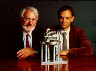
The development of the family of scanning probe microscopes started with the original invention of the Scanning tunneling microscope (STM) in 1981. Gerd Binnig and Heinrich Rohrer developed the first working STM while working at IBM Zurich Research Laboratories in Switzerland. This instrument would later win Binnig and Rohrer the Nobel prize in physics in 1986.
Gerd Binnig and Heinrich Rohrer
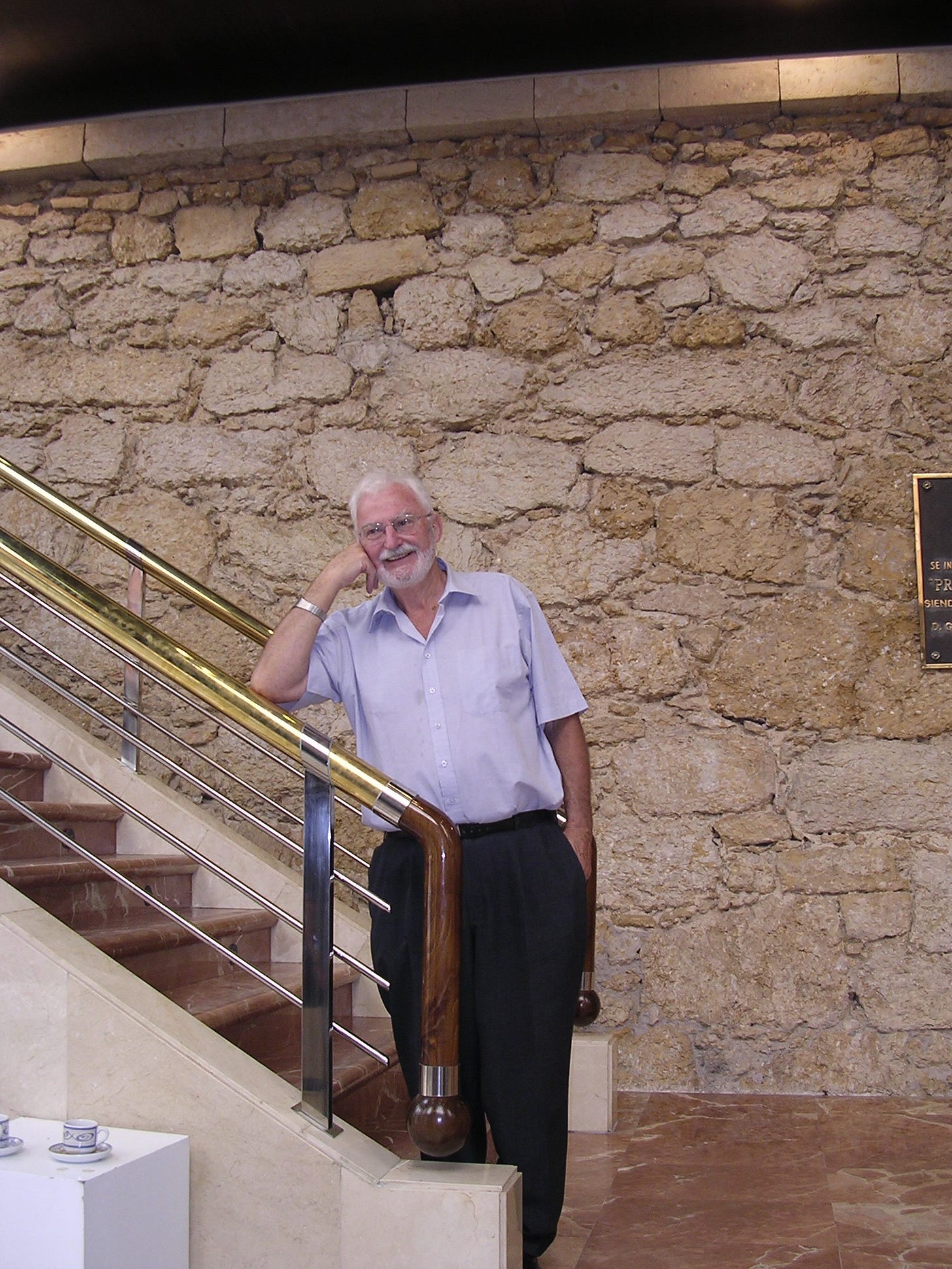
I had the opportunity to meet Heinrich Rohrer at the TNT2005 conference in Oviedo (Spain). The picture I show above is from my personal collection of pictures of the congresses we have done around the world. I remember that he had an exquisite treatment with everyone who wanted to talk to him. He told us that it had been a great conference. His presence made that event an interesting experience for all attendees.
The atomic force microscope (AFM) was developed to overcome a basic drawback with STM – it can only image conducting or semiconducting surfaces. The AFM has the advantage of imaging almost any type of surface, including polymers, ceramics, composites, glass, and biological samples.
Binnig, Quate, and Gerber invented the AFM in 1985. Their original AFM consisted of a diamond shard attached to a strip of gold foil. The diamond tip contacted the surface directly, with the interatomic van der Waals forces providing the interaction mechanism. Detection of the cantilever’s vertical movement was done with a second tip – an STM placed above the cantilever.
Binnig, Quate, and Gerber
What is the principle of atomic force microscopy?
AFM microscopes operate on the principle of surface sensing using an extremely sharp tip on a micromachined silicon probe. This tip is used to image a sample by raster scanning across the surface line by line, although the method varies dramatically between distinct operating modes. The two primary groups of operating modes are widely defined as contact mode and dynamic, or tapping, mode.
The underlying principle of AFM is that this nanoscale tip is attached to a small cantilever which forms a spring. As the tip contacts the surface, the cantilever bends, and the bending is detected using a laser diode and a split photodetector. This bending is indicative of the tip-sample interaction force. In contact mode, the tip is pressed into the surface and an electronic feedback loop monitors the tip-sample interaction force to keep the deflection constant throughout raster scanning.
Tapping mode limits the contact between the sample surface and the tip to protect both from damage. In this mode, the cantilever is caused to vibrate near its resonance frequency. The tip subsequently moves up and down in what is described as a sinusoidal motion. This motion is reduced by attractive or repulsive interactions as it comes near the sample. A feedback loop is used in a similar fashion to contact mode, except it keeps the amplitude of this tapping motion constant rather than the quasistatic deflection. By doing so, the topography of the sample is traced line by line.
The video, courtsey of PI (Physik Instrumente (PI) GmbH & Co. KG ), shows how parallel kinematic piezo stages enable superlative specimen positioning in Atomic Force Microscopy (AFM), Scanning Near-field Optical Microscopy (SNOM) and Confocal Raman Imaging. The subnanometer resolution, fast response times, highest linearity and excellent scanning flatness of multi-axis piezo positioners allow the combination of all three methods in one highly innovative nanoanalytical microscope system.
How small an object can an AFM clearly see?
The smallest thing that we can see with a ‘light’ microscope is about 500 nanometers. One nanometer is one-billionth (that’s 1,000,000,000th) of a meter. So the smallest thing that you can see with a light microscope is about 200 times smaller than the width of a human hair. Bacteria are about 1000 nanometers in size. The reason we can’t see anything smaller is because these microscopes use light. Normally, we don’t think about light as having a size, but visible light is about 500-800 nanometers. To see anything smaller we need a more powerful microscope.
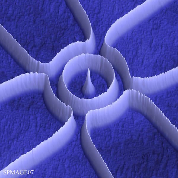
Courtesy - Andreas Fuhrer (Switzerland) & ICMM-CSIC (Spain)
Image Description:
The image shows a four-terminal quantum ring structure defined in a two-dimensional electron gas (2DEG) with local anodic oxidation using an atomic force microscope tip. The elevated white lines represent the oxide on the surface of the GaAlAs heterosstructure containing the 2DEG. These oxide lines are on average 15nm high and penetrate just as deep into the sample surface, forming barriers in the electron gas below. The ring has an average diameter of 1 micron and the four outer rectangular areas enclosed by oxide lines are used as in-plane gates to tune the electron density of the four arms of the ring. Measuring Aharonov-Bohm oscillations in the ring conductance this device is used to interferometrically detect the relative phaseshift of Coulomb blockade resonances in two quantum dots induced in the arms of the ring.
The atomic force microscope is one of the world’s most powerful microscopes. They don’t see things with light. Instead, they use a very sharp tip that looks like a needle to “feel” the surface of the object they are trying to see. Sometimes, scientists will put carbon nanotubes at the end of the sharp tip to make them even sharper. A carbon nanotube tip is so sharp, it is only a few atoms wide.
This tip is so sharp that as it is moved across something, the tip can feel the shape by measuring the forces between the atoms on the tip and the atoms on the object. Using powerful computers, all this information about the forces can be used to create a three-dimensional view of the object. With an atomic force microscope, you can see things as small as a strand of DNA. This is how scientists have been able to “see” DNA and show that it is truly double helix shaped like Watson and Crick showed over 50 years ago.
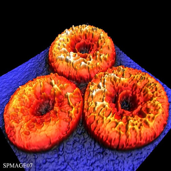
Courtsey: Luciano Paulino Silva (Brazil) & ICMM-CSIC (Spain)
Image Description:
Phyllomelittin is a novel antibiotic peptide isolated from the skin of the monkey frog Phyllomedusa hypochondrialis. It has been demonstrated that antibiotic peptides exert their activities by disrupting cell membranes. Therefore, the study of the effects of such peptides on cell membranes has been the focus of intense research efforts using the atomic force microscopy (AFM). The aim of this study was to investigate the surface of human red blood cells (RBCs) after treatment with phyllomelittin. The cells were deposited onto a glass slide (blue) and fixed with methanol for 5 minutes. The image shows the intermittent contact mode topography (14.5 µm x 14.5 µm x 819 nm) of three RBCs after 25 minutes of incubation with phyllomelittin at 32 µM. A large number of elevations of few nanometers (yellow) were found to be distributed heterogeneously on the RBCs surface (red), presumably reflecting the regions of the cell membrane disrupted by and/or interacting with phyllomelittin molecules.
What is atomic force microscopy used for?
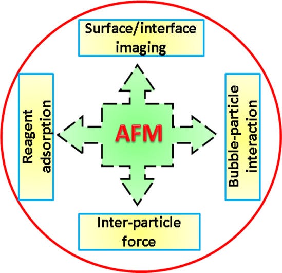
Atomic force microscopy (AFM) is a powerful technique that enables the imaging of almost any type of surface, including polymers, ceramics, composites, glass and biological samples. AFM is used to measure and localize many different forces, including adhesion strength, magnetic forces and mechanical properties. AFM consists of a sharp tip that is approximately 10 to 20 nm in diameter, which is attached to a cantilever. AFM tips and cantilevers are micro-fabricated from Si or Si 3N4. The tip moves in response to tip–surface interactions, and this movement is measured by focusing a laser beam with a photodiode.
An AFM is operated in two basic modes, such as contact and tapping modes. In the contact mode, the AFM tip is in continuous contact with the surface. In contrast, in the tapping mode, the AFM cantilever is vibrated above the sample surface such that the tip is only in intermittent contact with the surface. This process helps to reduce shear forces associated with the tip movement. The tapping mode is the recommended mode that is commonly used for AFM imaging. The contact mode is only used for specific applications, such as force curve measurements. The AFM is used to image and manipulate atoms and structures on a variety of surfaces. The atom at the apex of the tip ‘senses’ individual atoms on the underlying surface when it forms incipient chemical bonds with each atom. Because these chemical interactions delicately alter the tip’s vibration frequency, they can be detected and mapped.
Unlike the electron microscope, which provides a 2-D projection or a 2-D image of a sample, AFM provides a true 3-D surface profile. In addition, samples viewed by AFM do not require any special treatments (i.e. metal/carbon coatings) that would irreversibly change or damage the sample. Whereas an electron microscope requires an expensive vacuum environment for proper operation, most AFM modes can work perfectly well in ambient air. In principle, AFM can provide higher resolution than Scanning Electron Microscope (SEM) . It has been demonstrated that AFM can provide true atomic resolution in ultra-high vacuum (UHV) and, more recently, in liquid environments. High resolution AFM is comparable in resolution to scanning tunneling microscopy and Transmission Electron Microscope (TEM). A disadvantage of the AFM technique compared to the SEM is the image size. The SEM can image an area in the order of millimeters by millimeters with a depth of field in the order of millimeters. The AFM can only image a maximum height in the order of micrometers and a maximum scanning area of approximately 150 by 150 micrometers.
In the case of clay-containing polymer nanocomposites, AFM has been used to image the surface of clay particles dispersed in a polymer matrix. For example, Yalcin and Cakmak used AFM to image the surface morphology of the intercalated silicate layers dispersed in nanocomposite films.8 Recently, researchers have also been using AFM to investigate the effect of incorporating nanoclay particles on the morphology and crystal growth behavior of immiscible polymer blends.
What is the difference between SEM and AFM?
- AFM/SEM Differences: Composition
SEM also has a distinct advantage over AFM when it comes to determining the composition of a material. When the electron beam strikes a sample, a number of different signals are emitted, including back-scattered electrons, secondary electrons, X-rays, light and electrons. All of these signals provide different kinds of information.
X-rays and back-scattered electrons are the two most commonly used signals. X-ray emissions are created when electrons in the SEM beam strike electrons in the sample atoms. Using a spectrometer, scientists can use X-ray emissions to determine the elemental composition of a sample.
Back-scattered electrons are electrons from the beam being scattered out of the back of the sample. The number of back-scattered electrons from a sample has been determined to be based on the atomic number of the material. A detector can pick up these electrons and determine the make-up of a sample.
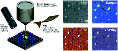
Courtsey of Group´s Séverine Le Gac (Applied Microfluidics for BioEngineering Research, MESA+ Institute for Nanotechnology and TechMed Center, University of Twente, The Netherlands)
Immuno-capture of extracellular vesicles for individual multi-modal characterization using AFM, SEM and Raman spectroscopy
AFM may not be able to provide any information on the elemental makeup of a sample, but it can determine a number of other compositional properties – including stiffness, elasticity, adhesion, magnetic and electrostatic fields, temperature distribution, spreading resistance, and conductivity. Some of these techniques involve the use of a magnetic or conductive probe tip, which can detect the attractive and repulsive forces between the tip and the sample.
Using a diamond tip on the AFM probe can also reveal details about a sample’s composition. The diamond tip can be used to scratch or make small indentations in the sample, revealing information about its properties.
- AFM/SEM Differences: Environment
One of the biggest differences in the way that the two techniques are carried out is the environment in which the tests are performed. SEM must be conducted in a vacuum environment, whereas AFM can be performed in a vacuum, ambient, gas or liquid environment.
This fact becomes particularly relevant in certain aspect of biology, where hydrated samples need to be tested. A special chamber can be set up to use SEM in these situations; however, this results in a loss of resolution.
In instances where a sample must be tested in a particular environment, AFM provides a distinct advantage. The technique is frequently used to image samples in liquid in an enclosed environment. AFM can also be used to test in gaseous environments, such as those involved in the development of polymers.
What kinds of observations can be made with atomic force microscopy?
An atomic force microscope (AFM) is a magnifying observation tool capable of measuring 3D textures of a minuscule area. Unlike scanning electron microscopes, it can acquire height data in numeric values, which enable quantification of sample and data post-processing. The AFM also allows for measurements in normal atmosphereic conditions and is free from restrcitions such as the need for sample pretreatment and electrical conductivity. On the other hand, however, it is subject to the limitation of a narrow measuring range (XYZ) due to its high-resolution capabilities. AFMs are also often unable to accurately position its probe to the measurement area and requires the need for knowledgable operation (proper mounting of the cantilever, etc.)
Don't hesitate to subscribe if you haven't already done so.
Regards and take care.
Born in 2012, Scixel is a project devoted to the improvement of the scientific comunication through the creation of graphical products: pictures, animations, graphs, posters, etc. Scixel consists of scientists with a deep knowledge in digital graphics but also with a long experience in giving talks, preparing posters and papers and other daily situations of scientific work.
We have focused our work into universities and research institutes all over the world: TuDelft (The Netherlands), NIMS (Japan), Basel University (Switzerland), Universidad Autónoma de Madrid, CNB or ICFO (Spain), to name a few.
Web: https://scixel.es/
If you are a company or an individual who would like to place your advertising in my newsletter you can contact me (email) and let me know your request of type of ad and number of newsletters you would like to place it. I will send you a budget as soon as possible.


